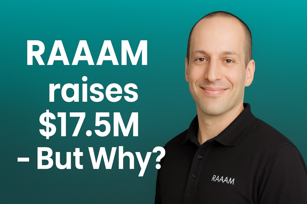
Israeli startup RAAAM Memory Technologies just closed an oversubscribed $17.5 million Series A funding round led by NXP Semiconductors. This brings their total funding to over $24 million, including earlier seed rounds and European Innovation Council grants. But why are major chip makers pouring millions into this company? The answer lies in solving one of the semiconductor industry’s biggest headaches—and the potential to transform how chips are built.
What Problem Does RAAAM Solve?
Modern chips face a critical memory bottleneck. On-chip memory now consumes up to 75% of total chip space in AI and machine learning applications. The industry standard SRAM uses six to eight transistors per bit, making it area-inefficient and difficult to scale below 10-nanometer process nodes. This creates a massive problem: chips need more memory, but SRAM takes up too much space and consumes excessive power. RAAAM’s GCRAM technology addresses this directly by storing data using only three transistors instead of six to eight, delivering 50% area reduction and 10 times lower power consumption compared to SRAM.
Where Will RAAAM Use the Funding?
The new funds will support full qualification of RAAAM’s patented GCRAM technology in leading-edge process nodes of several top-tier foundries. The company plans to migrate GCRAM to process nodes smaller than 5 nanometers and qualify it for mass production according to industry standards. RAAAM has already demonstrated silicon validation across multiple foundries including TSMC, Samsung, and STMicroelectronics. The funding accelerates partnerships with semiconductor companies and aligns GCRAM with customer product roadmaps for commercial deployment.
Who’s Backing RAAAM and Why?
NXP Semiconductors leads the Series A round, joined by a multinational networking corporation, IAG Capital Partners, EIC Fund, LiFTT, Alumni Ventures, and existing investors. Victor Wang, Vice President of Front-End Innovation at NXP, stated they’ve collaborated with RAAAM for several years and witnessed first-hand the potential of their on-chip memory technology. This strategic investment from a major chip manufacturer signals strong industry validation. The investor lineup combines financial backing with technical expertise and market access, positioning RAAAM for rapid commercialization.
What Makes GCRAM Technology Revolutionary?
GCRAM works as a drop-in replacement for SRAM without requiring additional fabrication steps or costs beyond standard CMOS manufacturing. The technology has been validated across Bulk CMOS, FD-SOI, and FinFET processes from leading foundries. GCRAM offers 50% silicon area reduction and up to 10 times reduced power consumption over SRAM while maintaining compatibility with existing manufacturing infrastructure. Semiconductor companies can either produce more chips per wafer, cutting costs, or increase on-chip memory capacity using the same die size—both improving performance and profitability.
What’s the Industry Response?
CEO Robert Giterman called the oversubscribed funding round with high-profile strategic and financial investors another sign of confidence in their revolutionary technology, promising to resolve the memory bottleneck in leading-edge AI chips. CBO Eli Leizerovitz stated the funding validates industry need for their technology, positioning them to accelerate engagements with leading semiconductor companies and foundries. The European Innovation Council selected RAAAM from 969 applicants across 17 countries for their €5.25 million grant, further confirming the technology’s strategic importance for competitive semiconductor capabilities.
What Are RAAAM’s Future Plans?
RAAAM aims to establish GCRAM as the new standard for on-chip memory in next-generation chips. The company targets full production qualification with top-tier foundries and expanding collaborations with major semiconductor manufacturers. With NXP already implementing GCRAM and other companies evaluating the technology, RAAAM positions itself at the center of addressing AI’s memory requirements. Their roadmap includes advancing GCRAM for sub-5-nanometer nodes where SRAM scaling becomes increasingly challenging, potentially capturing significant market share in automotive, AI, 5G, and high-performance computing applications.

My Name is Adarsh and I am Empowering startups with high-quality content at Startups Union and bridging the gap between brand stories.
